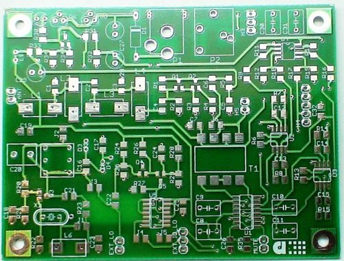
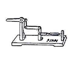
About PCB Designing Lab
Experience pristine performance with our PCB Designing Lab, a customizable and professional laboratory setup ideal for electronics, educational institutes, and R&D labs. Accommodating board sizes up to 300 mm x 400 mm and supporting single, double, and multi-layer designs, this hot deal offers world-class compatibility with Windows, Linux, and Mac. Featuring stellar speed (50-100 cm2/hr), accuracy (0.1 mm), and advanced HASL surface treatment, it ensures high-precision results. With CE-certified safety and user-friendly PC-based controls, this semi-automatic machine is supplied with essential accessories for prototyping excellence. Don't miss exclusive discounts from India's top distributor and manufacturer!
Application Scope and Key Features of PCB Designing Lab
Our PCB Designing Lab supports a wide surface of application, expertly handling FR4 and copper clad materials. Tailored for electronics innovation, academic training, and R&D prototyping, it excels in creating complex PCB layouts with multi-layer capability. Special features include a stellar user interface, precise 0.1 mm accuracy, HASL surface treatment, and compatibility with professional Gerber and DXF formats-perfect for demanding technical environments seeking reliability and ease of use.
Supply Coverage, Certifications, and Sample Policy for PCB Designing Lab
We maintain robust supply ability to accommodate bulk and custom requirements for distributors, exporters, and institutions. Shipped goods are CE certified, ensuring compliance with international safety standards. Express shipping options are available for urgent needs, and we offer a flexible exchange policy. Sample orders are encouraged for evaluation-demonstrating our commitment to client satisfaction and quick integration into your laboratory workflow, with seamless logistics support globally from India.
FAQ's of PCB Designing Lab:
Q: How does the PCB Designing Lab accommodate different operating systems?
A: The lab's system is compatible with Windows, Linux, and Mac operating systems, ensuring flexibility and seamless software integration across diverse technical setups.
Q: What is the maximum board size that can be processed in this lab setup?
A: The PCB Designing Lab can handle board sizes up to 300 mm x 400 mm, making it suitable for a variety of project scales in education, research, and prototyping.
Q: Where is the PCB Designing Lab most effectively utilized?
A: It is ideal for electronics prototyping in educational institutes, R&D laboratories, and professional workshops requiring reliable and precise PCB design capabilities.
Q: What special features make this PCB Designing Lab a hot deal for buyers?
A: Key features include customizable board options, high-precision accuracy (0.1 mm), multi-layer support, user-friendly PC-based controls, and compliance with CE safety standards-all at a competitive discount.
Q: How can purchasers benefit from the sample policy offered?
A: Buyers can request product samples to fully evaluate the lab setup before making larger commitments, ensuring it meets all application requirements and standards.


 Send Inquiry

 English
 Spanish
 French
 German
 Italian
 Chinese (Simplified)
 Japanese
 Korean
 Arabic
 Portuguese